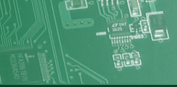
Home
Product Design
OverviewLeading Edge PerformanceCost ReductionAccelerated DesignsTurnkey Delivery
Services
OverviewFeasibility StudiesRF DesignAntenna DesignSoftware DesignMechanical DesignPCB DesignTest Fixture DesignAntenna TestingPre-compliance Testing
Technologies
OverviewBroadbandCellularTelemetrySpecialty
About Us
OverviewFacilitiesTeamPartnersProcessCareers
Contact Gallery

PCB Design


There are no more demanding layouts than the ones required for complex RF circuitry and many years of experience have taught us a detailed set of rules to follow. As the frequency of operation increases, the line between circuit design and layout becomes less and less distinct. Often the layout can be the most difficult part of the design.

  • Design for manufacturability
  • Design for durability in harsh environments
  • EMI suppression
  • Susceptibility
  • Cost efficiency
  • FR4, Getek, Duroid, ...

Using a comprehensive set of guidelines, Murandi can move your circuit design from schematic to printed circuit board efficiently.


Home Product Design Services Technologies About Us Contact Gallery

Copyright 2011 - Murandi Communications Ltd.